1.png)
I see that electronics assemblies require precise solder placement. Without the right approach, I waste time and money. I feel determined to find a solution that improves accuracy. Solder paste printing offers a stable, repeatable method to apply solder in various scenarios.
Solder paste printing technology applies controlled amounts of solder paste onto PCB pads, enabling consistent assembly, improved yields, and reliable solder joints.
I recall when I tried manual solder application1. Inconsistencies led to bridging and poor connections[^2]. After switching to solder paste printing[^3], defects decreased, and results improved.
[Table of contents]
- What is the application of solder paste?
- When should I use soldering paste?
- What is the function of solder paste printer?
- What is the process of solder paste PCB?
- Conclusion
- About My Business
- About My Typical Customers
What is the application of solder paste?
I remember the first time I used solder paste. Its thick consistency surprised me, but I realized it’s not just metal. It’s a blend of metal particles and flux designed for precise solder joints.
I apply solder paste onto specific PCB pads to form stable electrical and mechanical bonds after reflow, ensuring strong, reliable connections.
I once tried to place solder by hand. Without paste, the results were irregular and time-consuming. With paste, I gain consistency and confidence.

Defining the Purpose
Solder paste combines fine metal powders and flux. I print it onto pads where components sit. After heating, it melts and forms solder joints. This ensures parts stay firmly attached.
H3: Key Components of Solder Paste
- Metal Particles: Provide conductive pathways.
- Flux: Cleans surfaces and ensures proper wetting.
- Viscosity Modifiers: Control paste flow for printing.
Table: Paste Attributes and Benefits
| Attribute | Benefit |
|---|---|
| Controlled Viscosity | Ensures printing accuracy |
| Consistent Particle Size | Prevents bridging and voids |
| Balanced Flux Content | Enhances wetting and joint strength |
Aiding Assembly Processes
I find that solder paste streamlines PCB assembly. Automated printers deposit paste exactly where needed. This reduces manual labor and improves quality. Faster production and fewer errors become possible.
Matching Component Complexity
Modern electronics pack many tiny components. Solder paste printing helps align paste deposits with fine-pitch pads. It’s essential for high-density boards, where precision is key.
When should I use soldering paste?
I recall a time I wondered if solder paste was necessary for small repairs. I learned it’s best suited for production scenarios, especially when consistency and speed matter.
I use soldering paste when assembling complex boards, working with surface mount components, or needing consistent, high-quality joints at scale.
I remember how messy it was to manually solder dozens of tiny SMD resistors. After switching to paste, I saved hours and reduced scrap.
Identifying Suitable Conditions
Solder paste shines in scenarios that demand uniform solder volume. High-volume production lines rely on it. It’s less necessary for occasional one-off repairs, but ideal for mass assembly.
H3: Ideal Situations
- Surface Mount Technology (SMT): For reflow processes.
- Fine-Pitch Components: Small pads need precise paste.
- Prototype to Production: Easily scalable.
Choosing Paste over Wire
Solder wire needs manual application. It’s slow and prone to human error. Paste, delivered via stencil or jetting, ensures each pad gets the right amount, reducing the chance of bridging or insufficient joints.
Snippet paragraph for H2: I choose solder paste over solder wire when I need consistent, repeatable results on dense boards, improving efficiency and reducing manual errors.
I recall a colleague struggling with solder wires on a complicated board. After we introduced paste printing, his yield increased, and rework dropped significantly.
Ensuring Production Efficiency
Faster cycle times matter. Automated paste printing integrates into pick-and-place lines. This results in streamlined workflows and higher throughput, key to meeting tight deadlines.
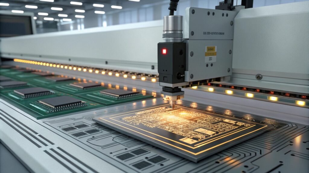
What is the function of solder paste printer?
A solder paste printer applies paste uniformly on PCBs. It’s a critical step before component placement. I rely on this machine for precise, repeatable printing patterns.
The solder paste printer’s function is to deposit an exact amount of solder paste onto PCB pads through a stencil, ensuring proper alignment and volume control.
I remember seeing my first solder paste printer in action. It was impressive how fast and accurately it worked, eliminating guesswork.
Achieving Precision Deposition
The printer aligns a metal stencil over the PCB. I spread paste across the stencil. The machine’s squeegees push paste into apertures. Removing the stencil leaves perfect deposits on pads.
H3: Printer Components
- Stencil: Defines paste patterns.
- Squeegee: Forces paste through apertures.
- Vision Systems: Align PCB and stencil accurately.
Controlling Volume and Placement
I adjust the printer’s settings to ensure the right amount of paste fills each aperture. Proper alignment prevents offset. I can tweak speed and pressure for optimal results.
Snippet paragraph for H2: The solder paste printer ensures each pad receives a consistent paste deposit by precisely controlling volume, placement, and alignment, improving solder joint quality.
Once, I tried printing paste manually. Results were uneven. Using a printer eliminated guesswork and standardized the process.
Table: Printer Adjustments and Effects
| Adjustment | Effect on Outcome |
|---|---|
| Squeegee Pressure | Influences paste volume |
| Print Speed | Affects paste distribution |
| Alignment Corrections | Ensures pad accuracy |
Streamlining the Workflow
The printer integrates into automated lines. After printing, the PCB moves to pick-and-place machines, then reflow ovens. This seamless flow reduces handling and errors, increasing productivity.
What is the process of solder paste PCB?
I think about the entire PCB manufacturing flow. Solder paste printing is one part, but it’s crucial. If paste application fails, everything else suffers.
The solder paste PCB process involves preparing the board, applying paste via a stencil printer, placing components, and then reflowing to form robust solder joints.
I remember explaining the process to a colleague. Once he understood the flow, he saw how small improvements at the printing stage affected final yields.
Step-by-Step Application
- Stencil Alignment: Line up the stencil over the PCB pads.
- Paste Deposition: Spread paste over the stencil.
- Squeegee Action: Press and draw paste across the stencil, filling apertures.
- Stencil Lift: Remove the stencil, leaving paste deposits.
- Component Placement: Place SMD components onto the paste.
- Reflow Oven: Heat until solder melts and forms joints.
- Inspection: Verify joint quality.
Snippet paragraph for H2: The solder paste PCB process involves printing controlled solder deposits on pads, placing components on this paste, and running through a reflow oven to create strong, reliable connections.
I recall watching this entire sequence. When done correctly, it feels seamless and efficient.
Ensuring Uniform Coverage
Uniform paste coverage prevents insufficient solder volume or bridging. By controlling paste thickness and stencil design, I achieve consistent results, reducing rework and rejects.
H3: Factors for Uniform Coverage
- Stencil Thickness: Determines paste volume.
- Aperture Design: Controls deposit shape.
- Stable Printing Parameters: Achieve repeatable outcomes.
Adapting to Board Designs
Every PCB differs. Complex layouts or unusual pad shapes may demand custom stencils. I work closely with stencil providers to ensure optimal geometry. This flexibility ensures solder paste printing adapts to new requirements.
Conclusion
Solder paste printing technology applies across multiple process scenarios, enabling precise solder deposition, improved efficiency, and reliable assembly outcomes. By understanding when and how to use solder paste, operating solder paste printers, and following the proper PCB process steps, I ensure stable and consistent results.
About My Business
My Name: Jony Yue
My Email: qiangyue@solderforce.com
Link to My Website: www.solderforce.com
Brand Name: SolderForce
Country: China
Products: Solder Paste Dispenser
Business Model: B2B
Status: I developed a solder paste piezoelectric jet valve that can be customized to specific requirements. It supports Gerber import, automatically generating dispensing instructions. I export mainly to India, North America, South Korea, Russia, and Vietnam.
Possible Client Identity: SMT factory procurement, electronics industry, photovoltaic industry, and electronics DIY enthusiasts. My products feature top quality, customizable logos, and unique styles. I promote through Alibaba and exhibitions.
About My Typical Customers
Name: Mark Chen
Country: India
Age: 40 years old
Characteristics: Mark buys for his company’s manufacturing line. He must meet stringent process requirements. He has no direct decision authority but influences choices.
Primary Purchase: Solder paste jetting equipment.
Buying Preference: Quality, compliance with process specs, and competitive pricing.
Status: Company owner and buyer.
Main Sourcing Locations: China.
Profit Model: Uses automation equipment to produce goods for clients.
How to Find Suppliers: Trade shows, Google searches.
Sourcing Key Points: Quality control, certification, logistics, and payment methods.
Pain Points: Slow overseas response times, delayed problem resolution. He understands sales but cares most about function and reliability.
-
Explains the process of applying solder manually and highlights its limitations, such as inconsistencies and defects. ↩